
The Results of Our Efforts
Grid Parity is Our Goal
We believe that through durable R & D investment and technology breakthroughs, Gold Stone will become one of the leaders of the photovoltaic industry. Our confidence is rooted in our restless technology innovations.



As the conductivity of the silicon film is poor, the TCO transparent electrode serves as a transition layer between metal electrode and silicon, which mainly reduces the recombination loss of the carriers when flowing on the surface of the parallel silicon wafer, increases the carrier collection efficiency, and also makes the metal electrode forms a good ohmic contact. In addition, TCO electrode also plays the role of anti-reflection. TCO transparent electrodes are generally required to have high transmittance, low resistivity.

Low processing temperature:The highest process temperature for producing HDT solar cells is less than 250ºC,meaning more energy saving in production;
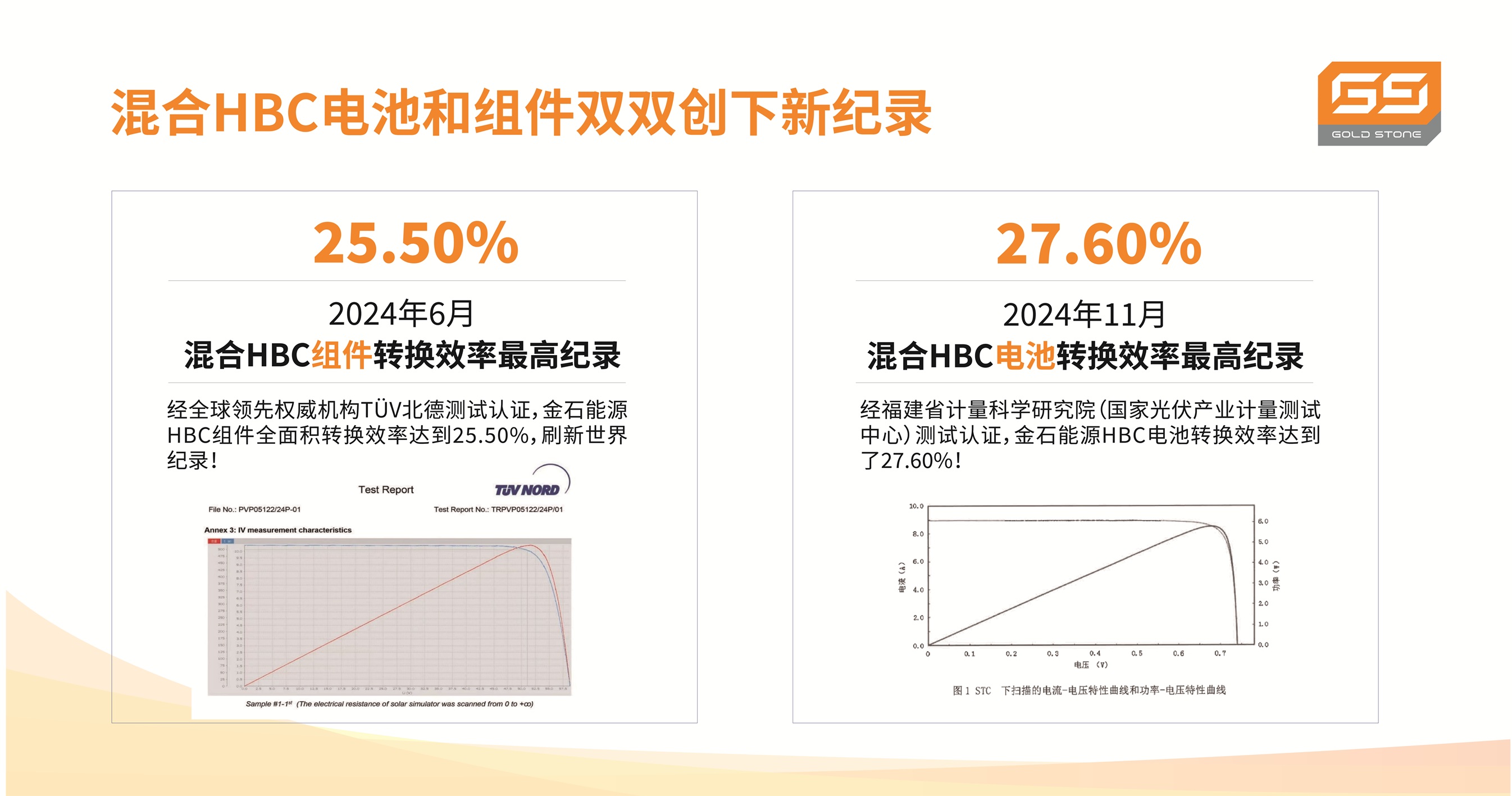
Hetero-junction emitter:Band engineering technology improves the quality of the amorphous silicon and widens its band gap, making the layer more transparent, resulting in the high short-circuit current (Isc) and high open-circuit voltage (Voc). The world record efficiency for this type of solar cells has reached to ~ 26.3%;
Low power-temperature coefficient:The power-temperature coefficient of HDT solar cell is less than ~-0.3%/ºC, making it more suitable working in hot outdoor environment.
Readiness of flexible solar cells technology:Gold Stone developed the technology to fabricate the very thin silicon solar cells. At this thickness, the solar cells are flexible, suitable for more practical applications;
Glass-glass module technology:HDT solar cells have a double-sided structure, which can receive the sunlight from both sides, well for making the glass-glass modules. With optimal positioning on the ground, the modules could generate ~10% more output power.

HDT solar cell contains a total of four layers of silicon film, in which P-type and N-type silicon doped layer as the emitter and back electrode field of the cell to build the internal electric field of the solar cell, with the thickness of about 5nm. The main role of the intrinsic silicon layer in the front and back of the monocrystalline silicon wafer is to passivate the surface of the monocrystalline silicon (Note: the surface of monocrystalline silicon due to the long-term structure of the crystal structure damage, resulting in a large number of surface defects), increase the minority carrier lifetime, and decrease the recombination of minority carrier on the interface. The intrinsic silicon layer of HDT solar cell has a thickness of 10nm or less, usually about 5nm. While in the traditional silicon thin film solar cells, the intrinsic silicon as the light absorption layer, the thickness is generally between 200nm ~ 300nm, the difference is about 50 times. Thus, the light-induced degradation effect in silicon thin film solar cells is recognized as not exist in HDT solar cells.
1、Reduction of Optical Loss:Reduce the textured surface reflection / Reduce the light absorption by TCO layer and amorphous silicon / Decrease the grid covering area by increasing its aspect ratio
2、Reduction of Surface Recombination Velocity:Improve the cleaning process for textured surface/Optimize the doping concentration of the doped amorphous silicon/Improve the quality of intrinsic layer
3、Reduction of Series Resistance:Increase the conductivity of TCO layer/Reduce the contact resistance between TCO layer and doped amorphous silicon
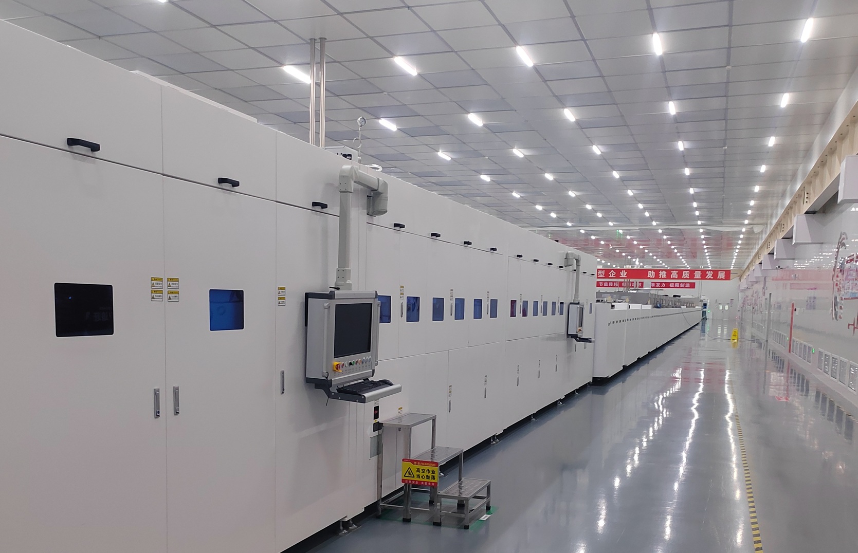
Improve the conversion efficiency of solar cells is one of the constant pursuit of photovoltaic industry goals. Based on heterogeneous silicon-based high-efficiency solar cell technology as a high conversion efficiency and low cost potential of the technical route, represents the development direction of the photovoltaic industry.
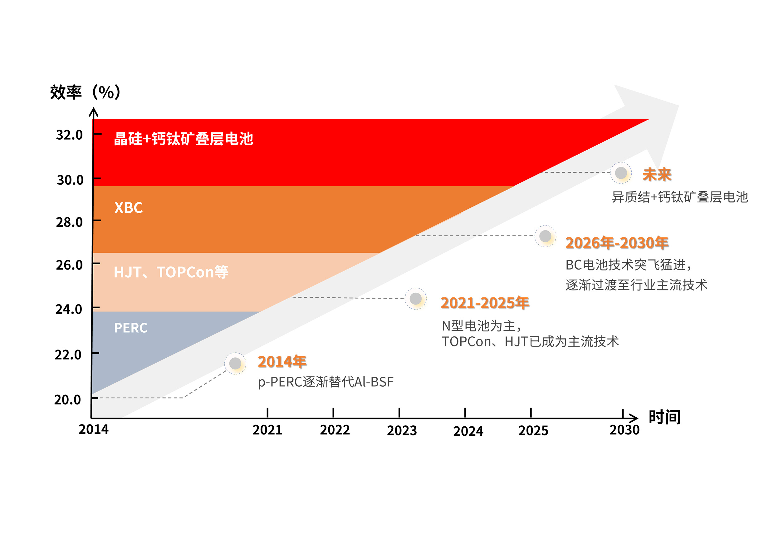
In-depth understanding of the photovoltaic technology development gives us a clear vision of where the photovoltaic industry is going.
Invest in R&D for future technologies, both mid-term and long term. Get ready for key technology innovations and upgrades in the photovoltaic industry.
Create new eco-system via vertical integration in the photovoltaic industry, further differentiating us from our competitors.
R&D Competence
Photovoltaic industry is growing exponentially and the competition in the industry is heated up.


